Tutorial — Practice 7: A/D converter
Learn by programming: follow each step, write your own code, then validate with the lab questions and exam. Adapt pins and routines to your board when needed.
What you will build
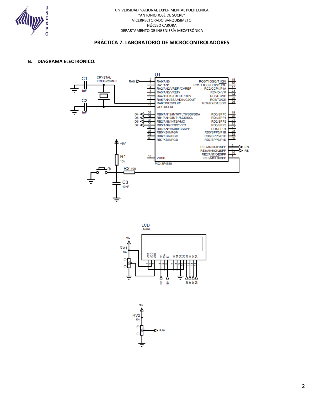
Read a potentiometer on AN0 with the ADC and display the value on LCD or LEDs.
-
1 Configure ADCON1, ADCON2, and ADCON0
ADCON1: RA0 analog (AN0), rest digital (`0x0E`). ADCON2: `ADCS = 101` (16 Tosc @ 20 MHz), right-justified result (`ADFM = 1`). ADCON0: channel AN0, `ADON = 1`.MOVLW 0x0E MOVWF ADCON1 MOVLW B'10100010' MOVWF ADCON2 MOVLW B'00000001' MOVWF ADCON0Tip: ADC theory: /en/adc/
-
2 GO/DONE read routine
Set GO = 1 to start conversion. Wait for GO = 0 (polling) or use ADIF interrupt. Read ADRESL and ADRESH → 10-bit value (0–1023).leer_adc: BSF ADCON0, GO espera: BTFSC ADCON0, GO GOTO espera MOVF ADRESL, W MOVWF adc_l MOVF ADRESH, W MOVWF adc_h RETURN -
3 Scale to voltage or percentage
With Vref = 5 V: `V = reading × 5 / 1024`. You can show integer mV or map to PWM. Use software division or a lookup table if it does not fit in 8 bits. -
4 Display the value on LCD
Reuse 4-bit LCD routines (Practice 2). Convert the number to ASCII digit by digit (`÷ 1000`, `% 10`, etc.) and write on line 2. Update each main loop pass. -
5 Calibrate with the potentiometer
Rotate the pot from 0 to Vcc and verify 0–1023 (or 0.00–5.00 V). If readings jitter, average 4–8 samples. Capture Proteus screenshot for the report.
Before you code — pre-lab
Pre-laboratory — reference research
Research for Practice 7 (A/D converter, UNEXPO). Links to course Topic 9.
Q 1 ADCON0, ADCON1 and ADCON2 registers
The PIC18F4550 10-bit ADC uses three registers:
| Register | Main role |
| --- | --- |
| **ADCON0** | Channel (`CHS`), ADC on (`ADON`), start conversion (`GO/DONE`) |
| **ADCON1** | Analog vs digital pins (`PCFG`) |
| **ADCON2** | Conversion clock (`ADCS`), result format (`ADFM`), acquisition time |
Typical flow: set ADCON1/ADCON2 once → select channel in ADCON0 → set `GO=1` → wait `GO=0` → read `ADRESH:ADRESL`.
Q 2 AN0 channel and potentiometer in the lab
The potentiometer divides voltage between VDD and VSS. The wiper connects to RA0/AN0. The digital value represents wiper position:
`V_in = (ADRES / 1023) × V_ref`
With `V_ref = VDD = 5 V`, ADRES = 512 ≈ 2.5 V. Set ADCON1 so RA0 is analog and other pins used by the LCD are digital.
Q 3 GO/DONE bit and conversion time
`GO/DONE` in ADCON0:
- Write 1 to GO → starts conversion.
- Hardware clears to 0 when done.
Time depends on ADCS (Tad) and acquisition time. At 20 MHz with ADCS = 101 (16 Tosc), Tad meets the datasheet minimum. Do not read the result while GO = 1.
With a 20 MHz crystal use ADCS = 101 (16 Tosc) in ADCON2 per the course guide.
Design your solution
Design before coding
The lab sheet asks for pseudocode and a flowchart before the .ASM. Write yours first, then unlock the reference guide.
- 1. Pseudocode
- 2. Flowchart
- 3. Reference
Write your pseudocode
Include: ADC register setup, GO/DONE wait, 10-bit read and LCD display routine.
0 characters (minimum 80)
Describe your flowchart
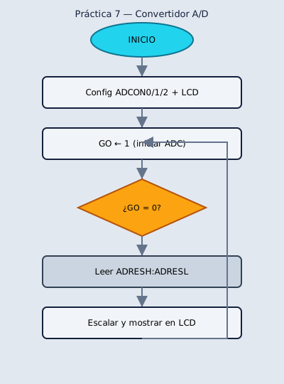
On paper or here: list each symbol in order. Your report needs ovals, rectangles, diamonds and the main loop.
0 characters (minimum 60)
My pseudocode draft
My flowchart draft
Reference pseudocode
START
    Configure ADCON1 (AN0 analog)
    Configure ADCON2 (ADCS=101, ADFM=1)
    ADCON0 ← channel 0, ADON=1
    Init LCD
REPEAT FOREVER
    GO ← 1
    WHILE GO = 1 DO ; wait
    value ← ADRESH:ADRESL
    voltage ← scale(value)
    display voltage on LCD
END REPEAT
Reference flowchart
Build and adapt the code
Practica · UNEXPO
Lab Practice 7
Implement analog-to-digital conversion: read a potentiometer or sensor, process the value, and display on LCD or LEDs.
Required steps in your code
Section titled “Required steps in your code”- Configure ADCON1 (analog pins)
- Configure ADCON2 (clock, format)
- Select channel in ADCON0
- Start conversion and wait for GO/DONE
- Read and scale to voltage or units
20 MHz crystal
Section titled “20 MHz crystal”Select ADCS = 101 (16 Tosc) in ADCON2 per Topic 9 ADC.
Reference source code
Section titled “Reference source code”After building — post-lab
Post-laboratory — reference research
Closing questions on ADC and display.
Q 1 Why right-justify the result (ADFM = 1)?
With ADFM = 1 (right-justified), the 10 useful bits sit in the low positions of `ADRESH:ADRESL`, making it easier to treat the value as a 16-bit integer. Left-justified format spreads bits differently and changes scaling code.
Q 2 Sources of error in ADC readings
Common errors: noise on the analog line (missing 100 nF on AN0), high impedance, unstable reference (noisy VDD), reading before GO = 0, or supply noise shared with the LCD. Mention at least two in your report and how you mitigated them.
Plot voltage vs ADRES in your report if possible.
Check what you learned
Exams by difficulty level
Open each level when you are ready. Basic is public; intermediate and UNEXPO levels require a CALETAS account to submit answers.
Basic Basic level — ADC and schematic 3 questions
ADCON registers and potentiometer on AN0.
0 of 0 answered
Sign in with CALETAS to sync this result across devices.
Sign in with CALETASIntermediate Intermediate level — Setup and scaling 3 questions
ADCON1/2, channel and voltage.
0 of 0 answered
Sign in with CALETAS to sync this result across devices.
Sign in with CALETASUNEXPO UNEXPO level — ADC oral 2 questions
Errors, ADFM and full conversion flow.
0 of 0 answered
Sign in with CALETAS to sync this result across devices.
Sign in with CALETAS