GPIO - TRIS, PORT and LAT
This page covers how to use TRIS, PORT, and LAT together in real code and UNEXPO labs. It builds on the ports guide and First LED — they come before this page in the sidebar and study path.
What GPIO is on the PIC18
Section titled “What GPIO is on the PIC18”GPIO (General Purpose Input/Output) means pins your program configures as digital inputs or outputs. On the PIC18F4550 you do not wire each pin separately to the CPU — you control ports: groups of 8 pins (A, B, C, D, E) through three SFRs per port.
Step 1 — Physical pin ↔ register bit
Section titled “Step 1 — Physical pin ↔ register bit”Each pin has a fixed hardware name:
| Pin | Port | Bit in TRISx / LATx / PORTx |
|---|---|---|
| RB0 | B | bit 0 |
| RB3 | B | bit 3 |
| RD7 | D | bit 7 |
Course rule: bit 0 = pin number 0. BCF TRISB, 0 affects only RB0; TRISB bits 1–7 do not change (Architecture — SFR).
Step 2 — Three registers, three roles
Section titled “Step 2 — Three registers, three roles”| Register | Write? | Purpose |
|---|---|---|
TRISx | Yes | Pin direction: 1 = input, 0 = output |
LATx | Yes | Output value in the internal latch |
PORTx | Read | Actual pin level (inputs, switches) |
Do not swap roles: TRIS first, then LAT for outputs or PORT to read inputs.
Step 3 — Typical program flow
Section titled “Step 3 — Typical program flow” Start / init_gpio ↓ TRISx — define inputs and outputs ↓ LATx — initial output state (LED off, etc.) main loop ↓ PORTx — read switches / buttons ↓ LATx — update LEDs / actuators ↓ GOTO loopIn sandwich style, init_gpio is usually a subroutine above; programa: calls CALL init_gpio and enters the loop.
Step 4 — How it fits with config bits
Section titled “Step 4 — How it fits with config bits”Config bits (PBADEN = OFF, LVP = OFF…) prepare hardware at power-on. GPIO registers (TRISB, LATB…) are configured while your code runs. If the LED does not respond, check both layers: crystal/FOSC and BCF TRISB, 0.
Registers per port — TRIS, PORT, and LAT
Section titled “Registers per port — TRIS, PORT, and LAT”| Port | Pins | TRIS | PORT | LAT | Course notes |
|---|---|---|---|---|---|
| A | RA0–RA5 | TRISA | PORTA | LATA | RA4 not analog; several pins can be ANx |
| B | RB0–RB7 | TRISB | PORTB | LATB | RB0 = INT0; RB4–RB7 = change interrupt |
| C | RC0–RC7 | TRISC | PORTC | LATC | RC6/RC7 = UART (TX/RX) |
| D | RD0–RD7 | TRISD | PORTD | LATD | LCD in labs |
| E | RE0–RE2 | TRISE | PORTE | LATE | Analog inputs RE0–RE2 |
All three registers share bit numbering: bit 3 of TRISB, PORTB, and LATB is always pin RB3.
Step 1 — Set direction with TRIS
Section titled “Step 1 — Set direction with TRIS”Before reading or writing, declare each pin as input or output.
One pin at a time (best while learning):
BCF TRISB, 0 ; RB0 → output (bit = 0) BSF TRISB, 3 ; RB3 → input (bit = 1)Whole port at once (Practice 1 — PORTB and PORTD as inputs):
MOVLW B'11111111' ; all bits = 1 → all inputs MOVWF TRISB MOVWF TRISDIn TRISx, 1 = input and 0 = output. If TRISB = 0xFF, all of PORTB is input — classic partial exam question.
More exercises in Set direction with TRIS.
Step 2 — Write outputs with LAT
Section titled “Step 2 — Write outputs with LAT”To drive an LED, relay, or digital line, write LATx, not PORTx:
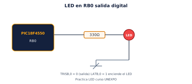
CLRF LATB ; clear all PORTB outputs BCF TRISB, 0 ; RB0 output BSF LATB, 0 ; RB0 high → LED ON BCF LATB, 0 ; RB0 low → LED OFFBSF/BCF on LATB touch one bit only — useful when inputs and outputs share a port (Bits and hex — masks).
Practical guide: Write outputs with LAT and First LED tutorial.
Step 3 — Read inputs with PORT
Section titled “Step 3 — Read inputs with PORT”For switches, buttons, or digital sensors, read PORTx:
BSF TRISB, 3 ; RB3 input BTFSS PORTB, 3 ; skip if RB3 = 1 (released, with pull-up) GOTO button_pressed ; jump → destination button_pressed: ; RB3 = 1 — button not pressed ... GOTO done_readbutton_pressed: ; RB3 = 0 — button pressed ...done_read:BTFSS PORTB, n / BTFSC PORTB, n are the most common course pattern. You can also MOVF PORTB, W and mask the bit (Bits and hex).
Practical guide: Read inputs with PORT.
Step 4 — PORT vs LAT — key difference
Section titled “Step 4 — PORT vs LAT — key difference”| Action | Correct register | Typical mistake |
|---|---|---|
| Turn on LED on RB0 | BSF LATB, 0 | BSF PORTB, 0 |
| Read button on RB3 | BTFSS PORTB, 3 | BTFSS LATB, 3 |
| Turn off all of PORTC | CLRF LATC | CLRF PORTC |
On pure outputs, writing PORTx sometimes “works” because it shares hardware with the latch, but in the course and datasheet the correct practice is LATx to write and PORTx to read.
Configure several pins at once
Section titled “Configure several pins at once”You want RB0–RB3 as outputs and RB4–RB7 as inputs:
MOVLW B'11110000' ; bits 7..4 = 1 (input), 3..0 = 0 (output) MOVWF TRISBEquivalent pin by pin:
BCF TRISB, 0 BCF TRISB, 1 BCF TRISB, 2 BCF TRISB, 3 BSF TRISB, 4 BSF TRISB, 5 BSF TRISB, 6 BSF TRISB, 7For TRIS, design the mask inverted vs what you want as output: output = 0, input = 1.
Analog pins and digital GPIO
Section titled “Analog pins and digital GPIO”Several PORTA/PORTB pins start as analog inputs if PBADEN = ON in config bits. For course digital GPIO use PBADEN = OFF in the CONFIG block (Config bits — PBADEN).
If you mix ADC and digital in one lab, set ADCON1 to declare which pins are analog and which digital — otherwise PORTx may read nonsense even when TRISx is correct.
Full walkthrough — LED on RB0
Section titled “Full walkthrough — LED on RB0”Minimal fragment linked to Assembly — LED example:
        LIST    P=18F4550        #include <P18F4550.INC>        CONFIG  FOSC = HS, WDT = OFF, LVP = OFF, PBADEN = OFF
        ORG     0x0000        GOTO    programa         ; jump to main
init_gpio:        CLRF    LATB        BCF     TRISB, 0         ; RB0 output        RETURN
programa:        CALL    init_gpioloop:        BSF     LATB, 0          ; LED ON        GOTO    loop             ; jump → destination loop: (above)
        END
Flow: config bits (hardware at power-on) → TRIS (direction) → LAT (output state) → simulate in Proteus with the .HEX from MPLAB.
Common mistakes
Section titled “Common mistakes”| Mistake | Symptom | Fix |
|---|---|---|
Write PORTx instead of LATx | Erratic output or odd reads | Use BSF/BCF/CLRF on LATx |
Skip TRISx setup | Pin does not behave as expected | Always TRIS before LAT/PORT |
PBADEN = ON without ADCON1 | Digital GPIO “dead” on RA/RB | PBADEN = OFF or configure ADCON1 |
| LED without resistor | Overloaded pin | 220 Ω or 330 Ω in series |
| Mix bit and pin | “Set bit 3 but watch RB0” | Bit n = pin Rn on the same port |
UNEXPO Practice 1 — how ports fit
Section titled “UNEXPO Practice 1 — how ports fit”Practica · Laboratory
UNEXPO Practice 1
PORTB and PORTD as inputs (operand switches). PORTC and PORTE as outputs (result LEDs). RA0 as a button to change operation. Implement add, subtract, multiply, OR, AND, XOR, complement, rotate, and software division. Before the lab, review the ALU guide if you use the PIC ALU.
Next step — buttons
Section titled “Next step — buttons”When a pin is an input with a push button, you need pull-up and debounce. That is Buttons, pull-up, and debounce.
Exam-style questions
Section titled “Exam-style questions”What does TRISB = 0xFF mean?
All of PORTB configured as input (every TRIS bit is 1).
Why write the LED on LATB and read the button on PORTB?
LATB controls the desired output of the latch; PORTB reflects the actual level on the pin — required for inputs with pull-up or external wiring.
What happens if you forget BCF TRISB, 0 before BSF LATB, 0?
RB0 may still be an input; the latch changes but the pin does not drive the LED correctly.
Ejercicio · Parcial
Trace the flow
In Proteus, change BSF LATB, 0 to BSF PORTB, 0 with RB0 as output. Does the LED behave the same? Note why the course prefers LATB.
GPIO and ports
Based on: Clase Tema 2 y 3 (1).pdf
0 of 0 answered
Sign in with CALETAS to sync this result across devices.
Sign in with CALETAS