Analog-to-Digital Converter (ADC)
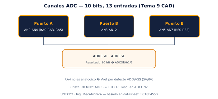
The PIC18F4550 has an integrated 10-bit ADC with 13 analog channels (AN0–AN12). It converts an analog voltage (potentiometer, LM35, resistor divider) into a digital number your program reads from ADRESH:ADRESL.
This page completes Topic 9 ADC: ADCON0/1/2 registers, conversion flow, and links to GPIO and config bits. The official lab is Practice 7 — A/D converter.
What the ADC does
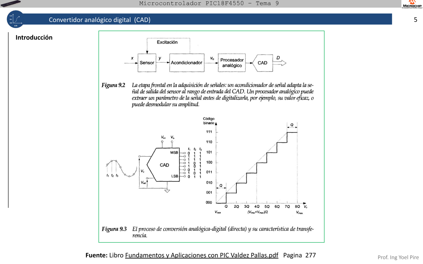
Section titled “What the ADC does”The A/D converter measures voltage on an analog pin and represents it as integer 0–1023 (10 bits).
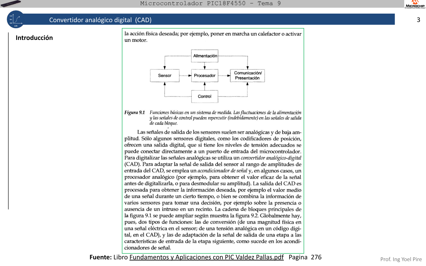
Step 1 — From analog world to digital
Section titled “Step 1 — From analog world to digital” Sensor (potentiometer, LM35…) ↓ voltage 0 V – Vref (typically 5 V) PIC ANx pin (RA0, RE0…) ↓ ADC module (successive approximation) ADRESH:ADRESL → value 0..1023 in your programStep 2 — Resolution and LSB
Section titled “Step 2 — Resolution and LSB”| Concept | PIC18F4550 value |
|---|---|
| Resolution | 10 bits → 1024 levels (0 to 1023) |
| 1 LSB | Vref / 1024 ≈ 4.88 mV with Vref = 5 V |
| Estimated voltage | V ≈ (ADRES / 1023) × Vref |
Example: ADRES = 512 → V ≈ 2.5 V with Vref = 5 V.
Step 3 — Three configuration registers
Section titled “Step 3 — Three configuration registers”| Register | Main function |
|---|---|
ADCON1 | Which pins are analog vs digital (PCFG) |
ADCON2 | Conversion clock (ADCS), format (ADFM), acquisition time |
ADCON0 | Channel (CHS), on (ADON), start/done (GO/DONE) |
Configure ADCON1/2 once at startup; each read touches ADCON0 (channel + GO).
Step 4 — Relation to GPIO and config bits
Section titled “Step 4 — Relation to GPIO and config bits”TRISx— ANx pin must be input.ADCON1— declares pin as analog; rest of port can stay digital (LCD, LEDs).PBADEN = OFFinCONFIG— avoids RA/RB starting as analog unintentionally (Config bits).
Analog channels AN0–AN12
Section titled “Analog channels AN0–AN12”| Port | Analog pins | Notes |
|---|---|---|
| A | RA0/AN0, RA1/AN1, RA2/AN2, RA3/AN3, RA5/AN4 | RA4 is not analog (T0CKI digital) |
| B | RB0/AN12, RB1/AN10, RB2/AN8, RB3/AN9, RB4/AN11 | Share port with GPIO and interrupts |
| E | RE0/AN5, RE1/AN6, RE2/AN7 | Common when LCD uses RE |
Practice 7: potentiometer on AN0 (RA0); LCD and control pins digital via ADCON1.
ADCON0 — channel, enable, and GO/DONE
Section titled “ADCON0 — channel, enable, and GO/DONE”| Field | Function |
|---|---|
CHS3:CHS0 | Selects channel AN0–AN12 |
ADON | 1 = ADC module on |
GO/DONE | 1 = conversion running; 0 = finished |
Read flow:
BSF ADCON0, GO ; start conversion ↓ Wait GO = 0 ; hardware done ↓ Read ADRESH:ADRESLADCON1 — analog vs digital pins
Section titled “ADCON1 — analog vs digital pins”PCFG in ADCON1 defines ANx vs digital GPIO. Typical Practice 7 — AN0 only analog:
MOVLW 0x0E ; RA0 analog, rest digital MOVWF ADCON1GPIO-only labs (Practice 1, keyboard LCD) often use ADCON1 = 0x0F for all pins digital.
ADCON2 — clock, format, and acquisition
Section titled “ADCON2 — clock, format, and acquisition”| Field | Function |
|---|---|
ADCS2:0 | Conversion clock (depends on Fosc) |
ADFM | 0 = right justified; 1 = left justified |
ACQT2:0 | Acquisition time (sample & hold) |
20 MHz crystal (UNEXPO course): ADCS = 101 in ADCON2. Reference code Practice 7:
MOVLW B'10100010' ; ADFM=1, ADCS=101 MOVWF ADCON2 MOVLW B'00000001' ; channel AN0, ADON=1 MOVWF ADCON0 BSF TRISA, 0 ; RA0 inputFull walkthrough — read AN0 (potentiometer)
Section titled “Full walkthrough — read AN0 (potentiometer)”Subroutines in sandwich style:
config_adc:        MOVLW   0x0E        MOVWF   ADCON1        MOVLW   B'10100010'        MOVWF   ADCON2        MOVLW   B'00000001'        MOVWF   ADCON0        BSF     TRISA, 0        RETURN
read_an0:        BSF     ADCON0, GO          ; start conversionwait_adc:        BTFSC   ADCON0, GO          ; skip if GO=0 (done)        GOTO    wait_adc            ; jump → loop until finished        MOVF    ADRESL, W           ; read result (per ADFM)        MOVWF   adc_l        MOVF    ADRESH, W        MOVWF   adc_h        RETURN
From programa:: CALL config_adc once; in loop CALL read_an0 and display on LCD or convert to voltage.
ADC interrupt (optional)
Section titled “ADC interrupt (optional)”You can use ADIE in PIE1 + PEIE + GIE to read the result in an ISR when ADIF sets — same chain as Timer1. Practice 7 usually uses polling on GO/DONE.
Common mistakes
Section titled “Common mistakes”| Mistake | Symptom |
|---|---|
| Skip ADCON1 | Erratic reads or LCD pins affected |
Pin as output (TRIS=0) | ADC does not measure correctly |
| GO without ADON | Conversion never starts |
| Wrong ADCS for Fosc | Slow or inaccurate conversion |
| Treat RA4 as analog | AN4 is on RA5, not RA4 |
UNEXPO Practice 7
Section titled “UNEXPO Practice 7”Practica · Laboratory
Practice 7 — A/D converter
Read a potentiometer or sensor on AN0, convert the value and show on LCD or LEDs. 20 MHz crystal: ADCS = 101 in ADCON2. Full tutorial: Practice 7.
Next step
Section titled “Next step”- PWM / CCP — another Topic 9 module (analog-like output via duty cycle)
- UART — send ADC value to PC (Practice 8)
- Partial IV — ADC + serial review
Exam-style questions
Section titled “Exam-style questions”How many bits does the PIC18F4550 ADC have?
10 bits → values 0–1023.
What does BSF ADCON0, GO do?
Starts a conversion; the bit stays 1 until done (GO/DONE = 0).
What is ADCON1 for?
Configures which pins are analog input vs digital GPIO.
Which PORTA pin is NOT analog?
RA4 — it is T0CKI (Timer0 digital input).
Ejercicio · Parcial
Calculate voltage
If Vref = 5 V and ADRES = 768, approximately how many volts? (768/1023 × 5 V)
A/D converter
Based on: Tema 9. CAD.pdf
0 of 0 answered
Sign in with CALETAS to sync this result across devices.
Sign in with CALETAS