Tutorial — Practice 1: Math operations
Learn by programming: follow each step, write your own code, then validate with the lab questions and exam. Adapt pins and routines to your board when needed.
What you will build
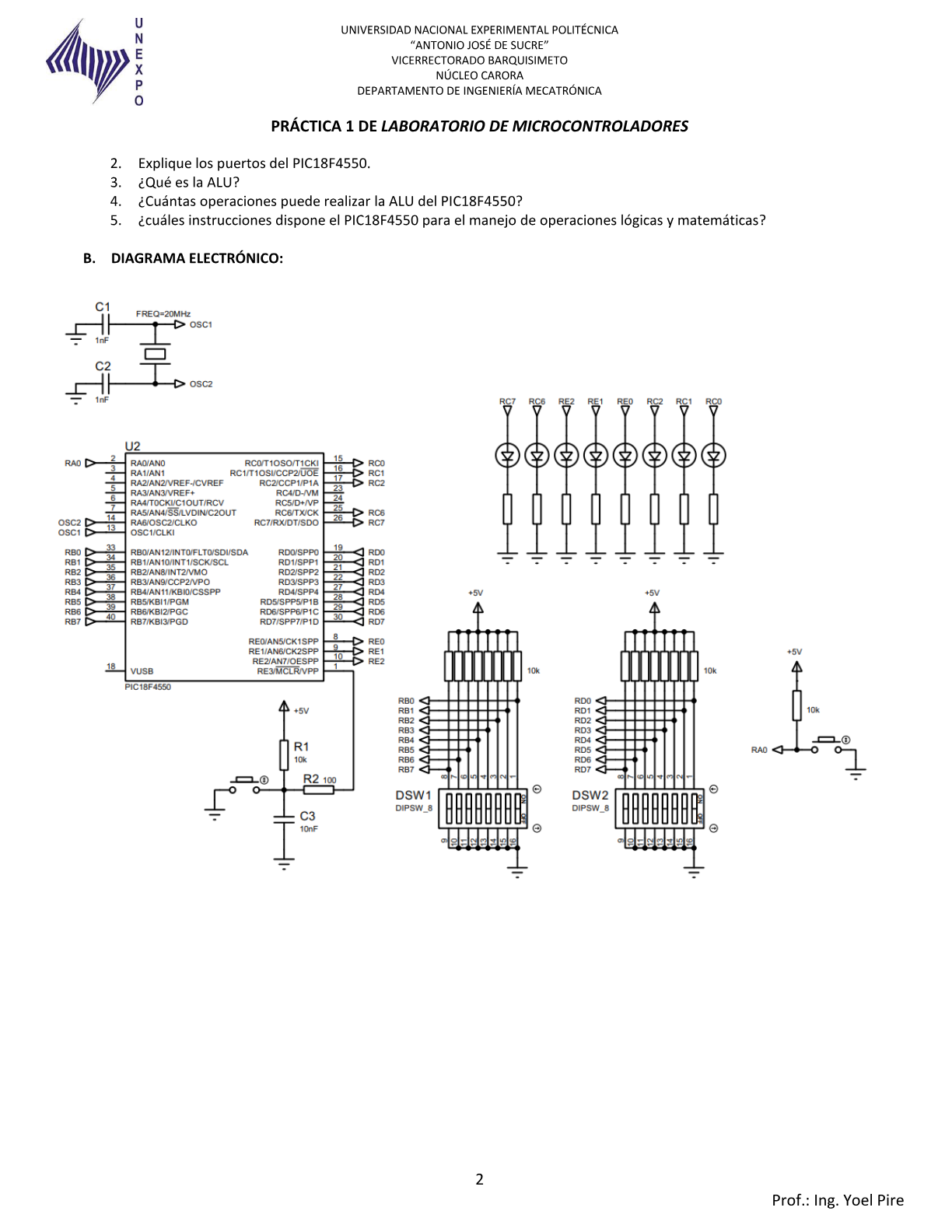
An ALU calculator with switches on PORTB/PORTD, result on LEDs, and operation change via RA0.
-
1 Wire the hardware per schematic
Operands on PORTB and PORTD (DIP switches with pull-up). Result on LATC and LATE (LEDs). Pushbutton on RA0 to change operation. Review the schematic before writing code. -
2 Configure port directions
RB and RD as inputs (`TRISB`/`TRISD` = 0xFF`). RC and RE as outputs (`TRISC`/`TRISE` = 0x00`). RA0 input for the button. Read operands with `MOVF PORTB, W` and `MOVF PORTD, W`.MOVLW 0xFF MOVWF TRISB MOVWF TRISD CLRF TRISC CLRF TRISE BSF TRISA, 0 ; RA0 entrada -
3 Implement one ALU operation
Start with add: `MOVF PORTB, W` → `ADDWF PORTD, W` → result in W → `MOVWF LATC`. Once it works, duplicate the routine for subtract (`SUBWF`), OR (`IORWF`), etc.suma: MOVF PORTB, W ADDWF PORTD, W MOVWF LATC -
4 Add multiply and software divide
`MULWF` leaves the product in `PRODH:PRODL`—display both bytes on RC and RE. Division has no native instruction: subtract the divisor repeatedly and count how many times it fits. -
5 Use RA0 to switch modes
Store the current mode in a RAM variable (`operacion`). Each press on RA0 increments the mode (0…8 then back to 0). In the main loop, branch to the routine matching `operacion`. -
6 Simulate, test on hardware, and document
Verify each mode in Proteus with different switch combinations. On the physical board, repeat tests. Complete the pre/post lab report with screenshots and an explanation of each operation.
Before you code — pre-lab
Pre-laboratory — reference research
Answers aligned with the official PDF (Practice 1, UNEXPO). Use them to guide your research: analyze them, expand with the datasheet, and write your report in your own words.
Q 1 Minimum system wiring for the PIC18F4550
The minimum system lets the PIC oscillate, reset and run on stable power:
- Power: VDD = +5 V DC and VSS = ground on the correct pins.
- HS oscillator (20 MHz): 20 MHz crystal between OSC1 and OSC2, with 1 nF capacitors from each crystal pin to ground (per the lab sheet).
- Reset (MCLR): 10 kΩ pull-up from MCLR to VDD, 10 nF from MCLR to ground, optional reset pushbutton from MCLR to ground.
- Programming: ICSP (PGC/PGD/MCLR/VDD/VSS) when using PICkit 2/3.
With CONFIG FOSC = HS the PIC uses the external crystal.
Q 2 Explain the PIC18F4550 ports used in this lab
This lab uses five ports with different roles:
| Port | Direction | Role |
| --- | --- | --- |
| **PORTB** | Input (`TRISB = 0xFF`) | Operand **A** — 8-bit DIP switch (RB0–RB7) |
| **PORTD** | Input (`TRISD = 0xFF`) | Operand **B** — second DIP switch (RD0–RD7) |
| **PORTC** | Output (`TRISC = 0`) | **Low** result byte on LEDs (RC0–RC7 → `LATC`) |
| **PORTE** | Output (`TRISE = 0`) | **High** byte for multiply (RE0–RE7 → `LATE`) |
| **PORTA** | RA0 input | Pushbutton to **change operation** |
Each digital port uses TRISx (direction), PORTx (read) and LATx (output latch). Switches use 10 kΩ pull-ups; LEDs use 220–330 Ω series resistors.
Q 3 What is the ALU?
The ALU (*Arithmetic Logic Unit*) is the CPU block that runs operations on register data: add, subtract, AND, OR, XOR, complement, increments, etc.
On the PIC18F4550 the ALU mainly works with WREG and data memory registers. It executes one instruction per cycle (except some two-cycle instructions). Results may land in WREG, a file register, or special pairs like PRODH:PRODL (multiply).
Q 4 How many operations can the PIC18F4550 ALU perform?
The ALU does not expose a fixed "mode count", but the PIC18 instruction set includes dozens of 8-bit arithmetic and logic operations, including:
- Arithmetic: add (`ADDWF`, `ADDLW`), subtract (`SUBWF`, `SUBLW`), inc/dec (`INCF`, `DECF`), multiply (`MULWF`).
- Logic: AND (`ANDWF`), OR (`IORWF`), XOR (`XORWF`), complement (`COMF`).
- Shifts/rotates: `RLCF`, `RRCF`, `RLNCF`, `RRNCF`.
Integer division has no dedicated PIC18 instruction and is done in software (repeated subtraction), as required in this lab.
Q 5 Which instructions handle logical and arithmetic operations on this MCU?
Instructions used directly in Practice 1:
| Lab operation | MPASM instructions |
| --- | --- |
| Add | `ADDWF` |
| Subtract | `SUBWF` |
| Multiply | `MULWF` → result in `PRODH:PRODL` |
| Divide (software) | `MOVF`, `SUBWF`, `ADDWF`, `INCF`, `BCF`/`BSF`, `GOTO` (loop) |
| OR / AND / XOR | `IORWF`, `ANDWF`, `XORWF` |
| Complement | `COMF` |
| Rotate, no carry | `RLNCF` |
Setup and control instructions include `MOVLW`, `MOVWF`, `CLRF`, `BCF`, `BSF`, `BTFSC`, `BTFSS`, `CALL`, `RETURN`, `GOTO` for port init, switch reads and operation selection.
Do not copy verbatim into your report. Your instructor expects your own wording, calculations and schematic. Use this guide to compare and improve your work.
Design your solution
Design before coding
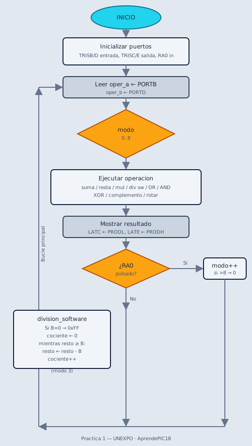
The lab sheet asks for pseudocode and a flowchart before the .ASM. Write yours first, then unlock the reference guide.
- 1. Pseudocode
- 2. Flowchart
- 3. Reference
Write your pseudocode
Include: port setup, main loop, CASE/SEGÚN for 9 modes, RA0 to change mode, software division routine.
0 characters (minimum 80)
Describe your flowchart
On paper or here: list each symbol in order. Your report needs ovals, rectangles, diamonds and the main loop.
0 characters (minimum 60)
My pseudocode draft
My flowchart draft
Reference pseudocode
START
    Configure ADCON1 ← digital
    LATC ← 0, LATE ← 0, mode ← 0
    TRISB ← 0xFF, TRISD ← 0xFF
    TRISA.0 ← 1, TRISC ← 0, TRISE ← 0
REPEAT FOREVER
    oper_a ← PORTB, oper_b ← PORTD
    CASE mode: add, sub, mul, div, OR, AND, XOR, NOT, rotate
    LATC ← low_byte, LATE ← high_byte
    IF falling_edge(RA0) THEN mode ← (mode+1) mod 9
END REPEAT
Reference flowchart
Build and adapt the code
Practica · UNEXPO
Lab Practice 1
Minimum PIC18F4550 system. Operands on ports B and D (switches). Result on ports C and E (LEDs). RA0 pushbutton changes the active operation.
Hardware map
Section titled “Hardware map”| Pin / port | Role in the program |
|---|---|
PORTB | Operand A (8-bit DIP switch) |
PORTD | Operand B (8-bit DIP switch) |
LATC | Result bits 0–7 (LEDs) |
LATE | Result bits 8–15 (LEDs; multiplication) |
RA0 | Pushbutton — cycles the active operation |
Included operations
Section titled “Included operations”Press RA0 to cycle modes (wraps to 0 after the last).
Reference source code
Section titled “Reference source code”Proteus / MPLAB
Section titled “Proteus / MPLAB”- Create an MPASM project for PIC18F4550 (20 MHz HS crystal).
- Use the practice schematic (PDF page 2).
- Switches on
RB0–RB7andRD0–RD7with 10 kΩ pull-ups. - LEDs on
RC0–RC7andRE0–RE7with 220–330 Ω resistors. - Pushbutton on
RA0to ground with pull-up.
After building — post-lab
Post-laboratory — reference research
Answers to the closing questions in the PDF. Use them as a starting point and add what you observed in Proteus or on hardware.
Q 1 What is the difference between a hardware operation and a software operation?
Hardware (native ALU): the PIC runs one instruction and the ALU returns the result in one or a few cycles. Examples: `ADDWF`, `SUBWF`, `MULWF`, `IORWF`/`ANDWF`/`XORWF`.
Software (algorithm): there is no single instruction; you write a routine. Example: integer divide — repeat subtraction while dividend ≥ divisor.
Orally: *"Addition uses ADDWF in hardware; division is our algorithm because PIC18 has no DIV instruction."*
Q 2 Why can you not always use all of PORTC as output?
Pins RC6 and RC7 have alternate functions (UART TX/RX). When EUSART is enabled, they are not simple GPIO. This lab uses `TRISC = 0` because UART is not used, but your report must explain that not every pin is a dedicated GPIO at all times.
In your final report add your own conclusions about PIC18 limits (8 bits, software division, pins shared with UART).
Check what you learned
Exams by difficulty level
Open each level when you are ready. Basic is public; intermediate and UNEXPO levels require a CALETAS account to submit answers.
Basic Basic level — Lab brief review 4 questions
Straightforward questions about the schematic and lab description. Good before the lab session.
0 of 0 answered
Sign in with CALETAS to sync this result across devices.
Sign in with CALETASIntermediate Intermediate level — Ports and ALU 4 questions
TRIS/LAT/PORT registers, ALU and arithmetic instructions. Report-style questions.
0 of 0 answered
Sign in with CALETAS to sync this result across devices.
Sign in with CALETASUNEXPO UNEXPO level — Code and oral exam 10 questions
Professor-style questions: line-by-line .ASM analysis, registers, memory and instructions.
0 of 0 answered
Sign in with CALETAS to sync this result across devices.
Sign in with CALETAS